Monte Carlo Simulation of Ionizing Radiation
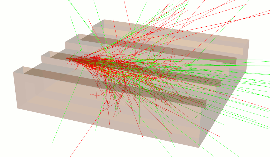
We do all kinds of computer simulation about ionizing radiation, like radiation damage, radiation detection, radiation protection and radiation dosimetry, mainly by Monte Carlo (MC) simulation.
There are plenty of free MC code packages, why do you still need us?
Why You Still Need Us
People are saying that MC simulation is simple, it's just about counting numbers. Yes, MC simulation is just about counting numbers, it's very simple, so simple that it's not ready for your engineering needs yet. It demands sophisticated users.
Accuracy
If your MC simulation isn't accurate, don't question the MC tool, question the way you are using it. What does it need to simulate accurately?
- An accurate physics and geometry modeling
- Appropriate variance reduction techniques
Accessibility
For most free MC program packages, there are almost no good graphical user interfaces. One may need sufficient software skills to use these free packages.
Dedicated to Your Needs
Most of the free MC simulation program packages are generally purposed. They can do everything, thus they can't do anything for you. Because they have no understandings of your needs.
Combination with Other Physical Processes
Your engineering tasks may need not only radiation simulation, but something else, like charge carriers simulation, for example. Thus MC simulation isn't enough for your tasks. You need other tools.
What You can Do with Cogenda
Dedicated Software
For your own engineering needs, Cogenda can write dedicated software for you.
- Combination with other computation methods for multi-physics problems;
- Parallel computation;
- Graphical user interface for easy use;
- Post-script interface for efficiency;
- Supporting multiple platforms.
Develop Your Own Software
If you want to develop your own simulation software, you need some basic physics and mathmetics function libraries. Cogenda has professional experience on these fields.
Solving Problems of Radiation
If what you want is a director answer, just contact us.
Examples
Example 1: SEE Fully Physical Simulation (Main Article)
Fully physical simulation of SEE is a combination of energetic particle transport simulation and charge carrier transport simulation. What we do includes:
- 3D modeling of the device;
- MC simulation of energetic particle using Geant4 package;
- TCAD simulation of carrier transport using Genius;
- An improved subset-simulation algorithm to reduce the computation cost
Example 2: Semiconductor Detector for Ionizing Radiation (Application Example for Download)
Similar to SEE simulation mentioned above, the simulation of semiconductor detector is also the combination of MC energetic particle simulation and TCAD charge carrier simulation. The work flow of the solution is shown as following figure:

Example 3: Dielectric Charging
When energetic electrons penetrate in dielectric material, the material will be charged, resulting in electric field inside it. The simulation work flow is shown as following figure:

-
WebTCAD

WebTCAD is the web version of Cogenda's VisualTCAD, a powerful tool of TCAD process and device simulation. It's mainly designed for teaching purpose, aimed at demonstrating/simulating industry-standard semiconductor fabricating and working process. The intuitive graphic UI, step-by-step workflow, and fully featured post process ability make it much easier for university teachers and students to use.
-
信息更新
- VisualTCAD 2024.10 released [2024-11-04]
- VisualTCAD 2024.06 released [2024-07-18]
- VisualTCAD 2024.03 released [2024-04-09]
- VisualTCAD 2024.02 released [2024-03-05]
- VisualTCAD 2023.12 released [2024-01-17]
- VisualTCAD 2023.11 released [2023-12-07]
- MozzTCAD 2023.10 released [2023-11-06]
- VisualTCAD 2.2 3D device simulator Genius support stress induced multi-valley mobility model for Si and SiGe material. [2022-11-01]
- VisualTCAD 2.1-p4 Simulation speed of 3D device simulator Genius increased by 10%~30%. [2022-08-24]
- VisualTCAD 2.1 3D device simulator Genius support nanometer device such as FDSOI and FinFET. [2022-05-15]
- VisualTCAD 2.0 First release of 2D process simulator Genes after years of development. [2021-10-17]
- Vspice 2.2 released [2019-4-15]
- Vspice 2.0 released [2018-10-20]
- VisualTCAD 1.9.2-3 Comes with revamped Total-Ionizing Dose effect simulation and supports SEE simulation in FDSOI circuits. [2017-10-15]
- Cogenda partners with POLYTEDA to distribute PowerDRC/LVS in Asia. [2017-9-15]
- Vspice 1.0 released [2017-4-15]
- CRad's FREE on-line version ForeCAST is open to you now! [2015-12-15]
- VisualTCAD 1.8.2-6 Comes with Total-Ionizing Dose effect simulation, among other improvements. [2015-7-10]
- Cogenda presented a quantitative analysis on the SEU rate of radiation-hardened SRAM cell due to elastic collisions at NSREC 2014. [2014-7-28]
- VisualTCAD 1.8.0-1 released with a new product for space radiation environment and effects analysis [2014-3-22]
- Cogenda presented a fully-physical simulation framework for single-event effects in semiconductor devices at RADECS 2012 [2012-9-28]
- Cogenda to present the super large TCAD device simulation at SISPAD 2012 [2012-6-18]
- Technical: Half-implicit solver for million-mesh-node TCAD device/circuit simulation [2012-6-18]
- VisualTCAD 1.7.4 released [2012-6-3]
- VisualTCAD 1.7.3 released [2012-1-1]
- VisualTCAD 1.7.2-5 released [2011-09-29]
- Cogenda to present MOSFET inverse-modeling technology at SISPAD 2011 and the companion workshop. [2011-07-17]
- Technical: Crossing the 10-transistor barrier of device simulation. [2011-07-12]
- New product: VisualParticle/GSeat for radiation effect analysis. [2011-07-01]
-
FinFET Transistor
FinFET devices are used in the latest 22nm generation CMOS processes. Construct your FinFET model with Gds2Mesh and simulate it with Genius, today.

